Partecipants: Marco, Matteo
In addition to the ADF4002 phase frequency detector evaluation board we design an external board to perform both the fast loop that acts on the Laser PZT and the slow loop that acts on the Laser PLT.
Description of the external circuit
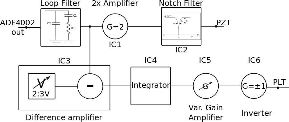
Attached: Fig 'boardblockscheme.png' shows the block scheme of the board and Fig '8.pdf' is the board electrical scheme.
The board mounts the loop filter (see entry 837 ) and 6 Op-Amps:
Loop Filter
C1 = 33nF, C2=680nF, R=27 Ω
Fast loop (PZT) input loop filer output
- IC1 is a 2x non-inverting amplifier (with the aim to amplify the correction signal from 0-5V to 0-10V)
- IC2 is an active notch filter with center frequency 270kHz. Fig 'pllnotchcharacterzation.pdf' represents the notch filter magnitude transfer function.
Slow loop (PLT) input loop filter outout
- IC3 is a difference amplifier in order to center arond zero V the loop filter output. The 2.5V offset can be tuned from 2V to 3V acting on a trimmer,
- IC4 is an integrator with a zero around 2Hz
- IC5 is a variable gain non iverting amplifier (gain from 1/2 to 1/5000)
- IC6 is an inverter to change the slow loop sign
Loop performances
We lock both the loop on PLT and PZT and measure the loop performances. The PLL servo loop was closed acting on AUX2 laser as slave laser.
Concerning the long term stability the PLL remains locked between Friday evening and Monday morning.
Concerning the loop phase noise I measured the PLL output phase noise between 100Hz and 102.k kHz with different charge pump gain. The used gain, the rms phase noise and the approximative loop bandwidth are reported in the following table:
| CP Gain [mA] | r.m.s phase noise [mrad] | Approx. loop bandwidth [kHz] |
| 1.875 | 8.67 | 30 |
| 2.5 | 7.78 | 36 |
| 3.125 | 6.56 | 38 |
| 3.75 | 5.13 | 43 |
| 4.375 | 4.53 | 49 |
| 5 | 3.96 | 53 |
Fig. 'phasenoisevsgain.pdf' shows the ouptput phase noise in the different configurations of the table above.
Fig 'phaenoisecp5mA.pdf' shows the phase noise and its cumulative rms value of the final configuration CP Gain = 5mA.