Marc and Yuhang
The first test of DDS3 board showed problem about USB connection. Therefore, we checked the connection and soldering of USB. We found a soldering problem related to USB connector. After that, we tried to solder it again. Following problems about soldering cost us quite a lot of time:
1. The wires going through the breadboard holes are not straight, which make wires very diffcult to be removed
2. A relatively large hole needs to be soldered in order to fix USB on the breadboard. When the solder is applied to an inappropriate side of this large hole, it causes the USB outer shell touching ground. We checked a working DDS board, whose USB's outer shell is not connected to ground. Due to this inappropriate solder, we wasted a USB connector.
3. When fixing USB on the breadboard, we need to choose the two sides of the breadboard. But only one side will make a correct connection.
After solving these problems, we tested DDS3 board output signal magnitude and put attenuator to get required level of signals.
DDS3 CH0: DDS output+18dB amplifier+12dB attenuator = -2dBm output (for PLL CC)
DDS3 CH1: DDS output+18dB amplifier+12dB attenuator = -2dBm output (for PLL ppol)
DDS3 CH2: DDS output+18dB amplifier+power splitter = 7dBm output *2 (for CC1 and CCFC)
DDS3 CH3: DDS output+18dB amplifier+10dB attenuator = 0dBm output (for CC2)
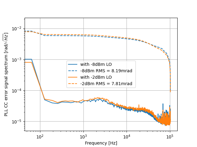
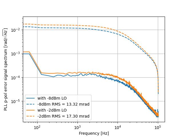
We compared the PLL phase noise for the cases of using -8dBm LO and -2dBm LO. From the datasheet of ADF4002, it requires LO from -5dBm to 2dBm. Therefore, we should prefer -2dBm LO. Figure 1 and 2 show the comparison of PLL phase noise. However, the shape of phase noise curve is not in agree with the measurement done in elog863, which needs further investigation.
On the other hand, higher LO also makes a higher phase noise. This is out of our expectation.