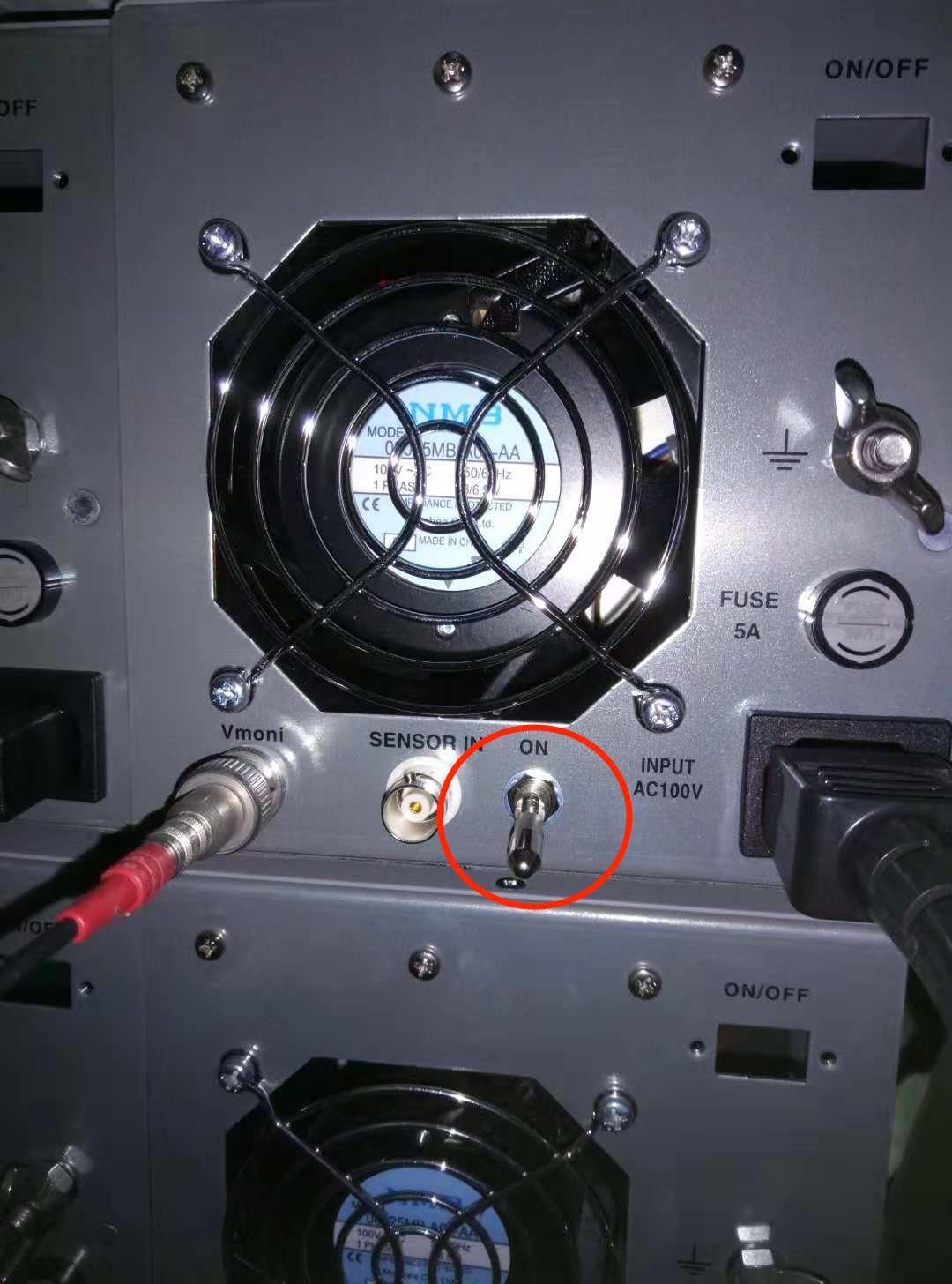
While we were using high voltage driver, we found the monitor channel give a highly distorted signal. At the begining, we thought it is the common issue of high voltage deriver. However, I just found out on yesterday that this distortion is caused by a switch on the rear panel of high voltage driver. See attached figure 1, the function of switch is to switch the sensor signal on or off. The switch is marked with a red circle in the picture.
The phenomenon is confirmed by me and like this. When you switch it on, you will see the distortion. When you switch it off, you will see almost the same with the ramp input. This is quite easy to confirm. But the question is whether it change the real output or not?
Firstly, I did the simulation of how our high voltage driver can affect the ramp signal.
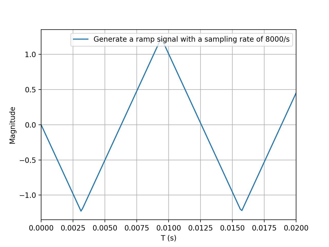
1. I generate ramp signal(80Hz) in time. I use additive synthesis to approxiamte our ramp signal. It is the summing of the odd harmonics of fundamental while every other odd harmonic multiplied by -1. Then multiply the amplitude of the harmonics by one over the square of their mode number.(more details in en.wikipedia.org/wiki/Triangle_wave#Definitions) See attached figure 4. We can see the ramp signal is quite decent.
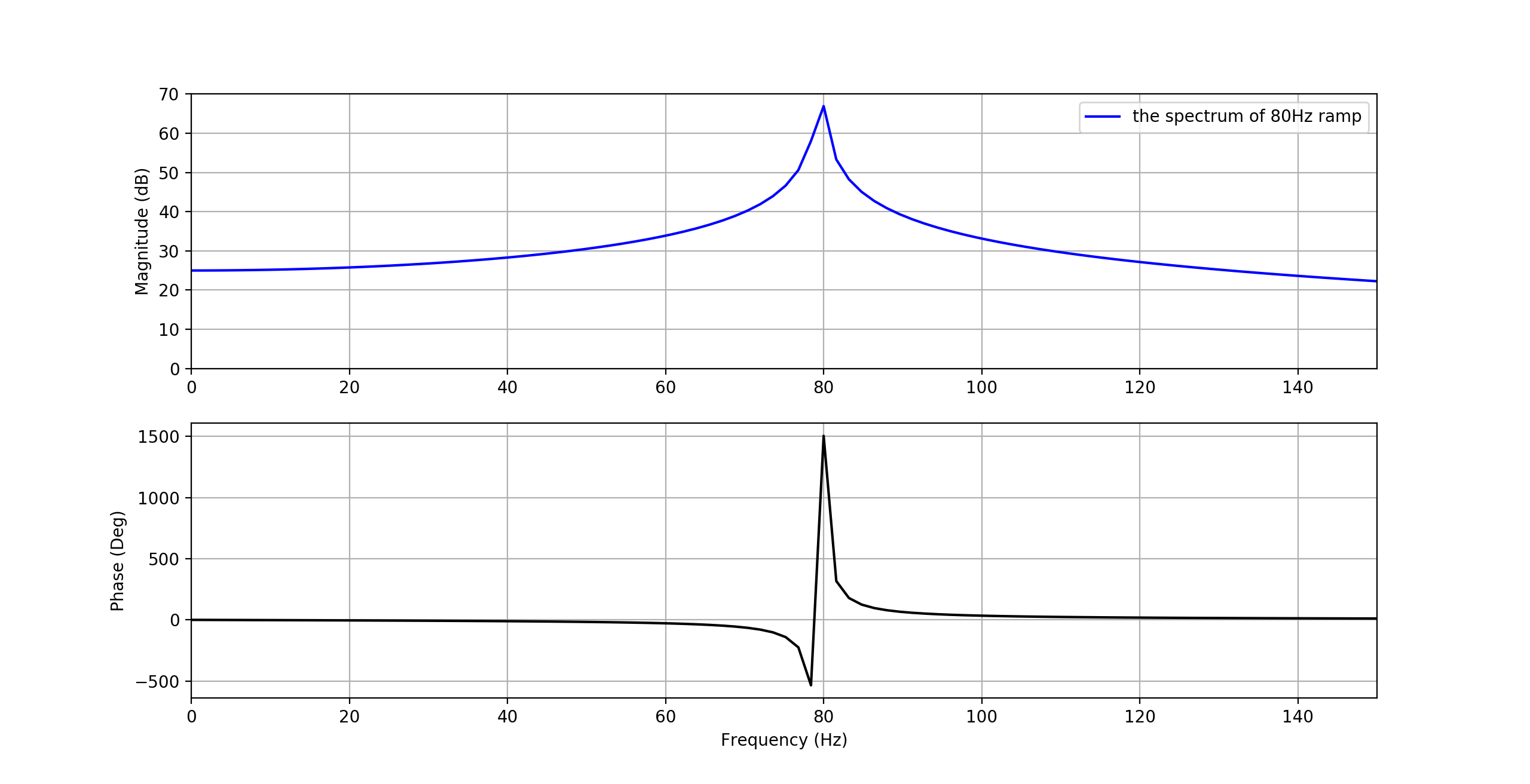
2. Use FFT to convert time-domain ramp into frequency-domain. See attached figure 5. It shows the spectrum of ramp signal. We can see a clear peak at 80Hz. (Actually there are some harmonic peaks of 80Hz, but they have much lower amplitude and at much higher frequency. So I didn't show them.)
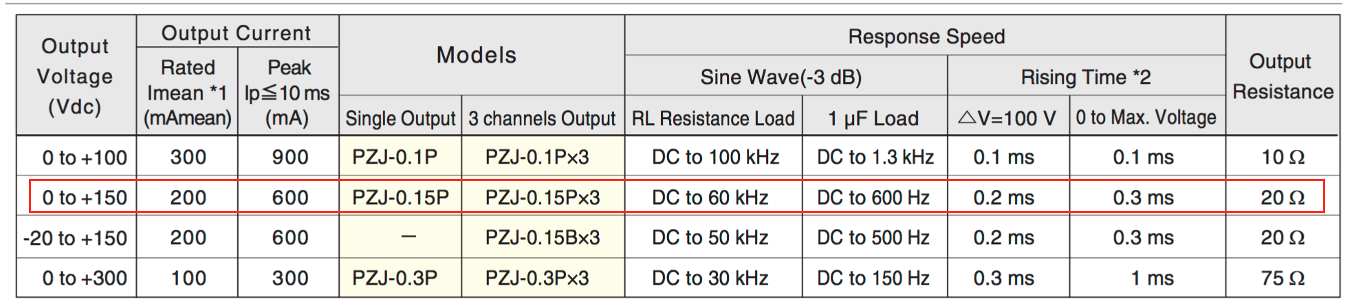
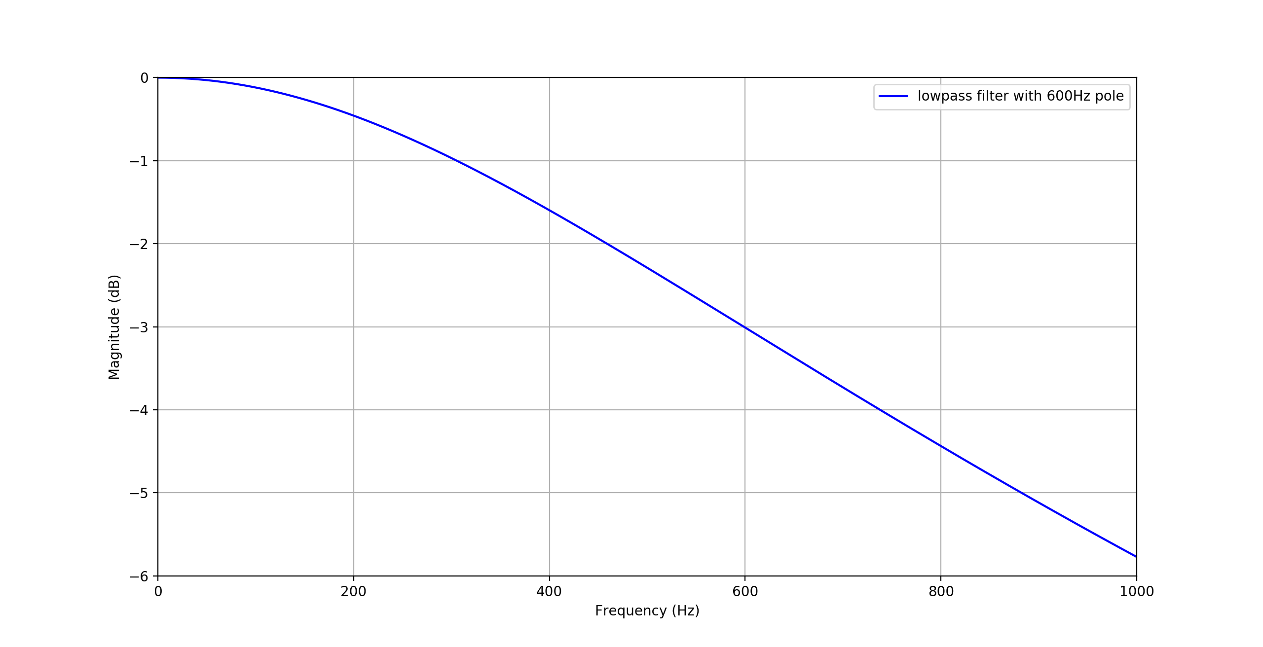
3. Apply the low pass filter of our high voltage driver. The corner frequency is shown in the datasheet of high voltage driver. See attached figure 2 and 3. Since our piezo's inductor is close to the data in the sheet, so we can use the value of 600Hz as pole. See attached figure 6. It shows the lowpass filter I applied.
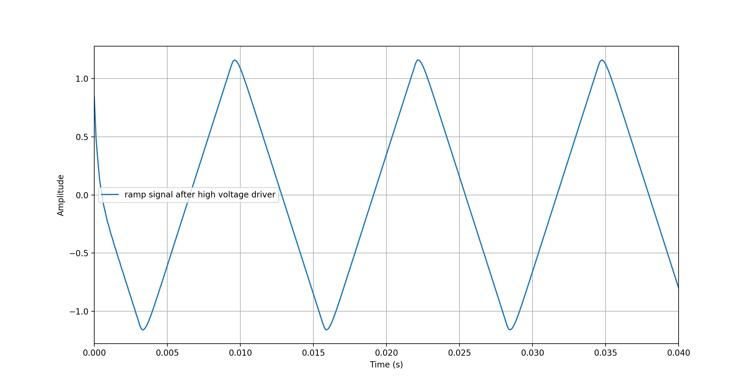
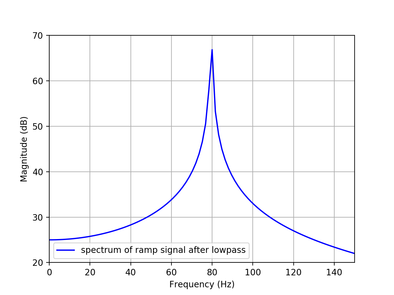
4. Convert frequency signal back to time domain. The result is shown in attached figure 7. You can see the distortion is not sever. And the frequency or amplitude almost remain the same. From the attached figure 8, you can see much better the frequency is exactly the same with before(80Hz).
So the comclusion of simulation is that high voltage driver should not change the ramp. The change is very trivial.
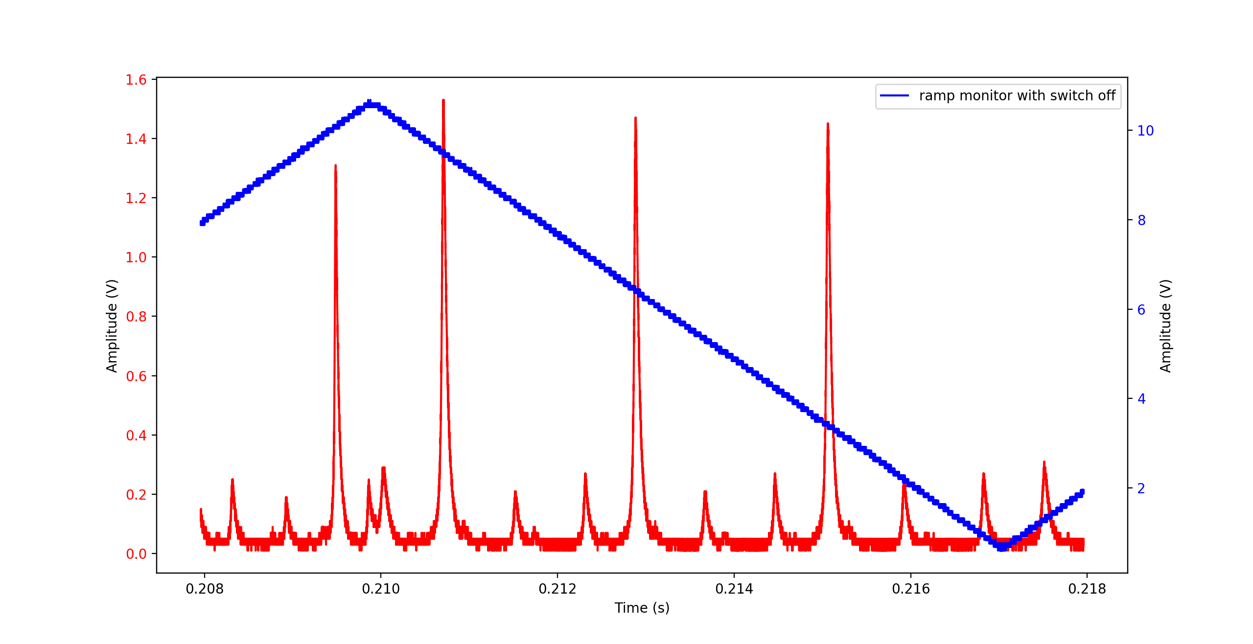
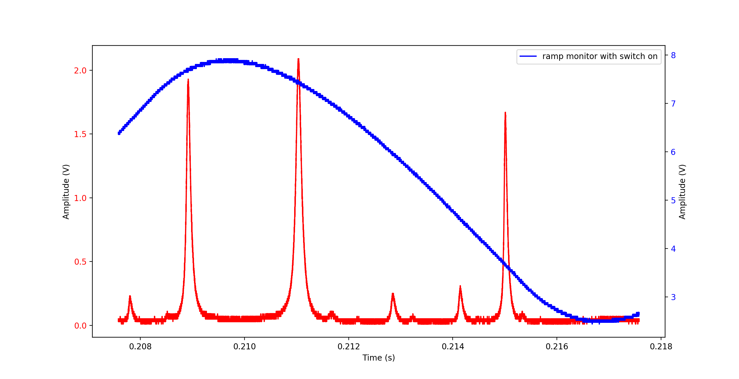
Then I checked the situation of this ramp output by looking at the scanning of OPO cavity. Figure 9 shows the scanning while the switch is off. We can see we have three TEM00. However, after I switch it on the sensor in port. I got the result of figure 10. No matter how I change the offset of high voltage driver, I can see only two TEM00. So this means the switch really changes the output of high voltage driver.
Unfortunatly, I found the switches are on for SHG's, GRMC's and IRMC's high voltage driver. So in the future, we need to take care not switch on the 'sensor in switch'. And also, for the low frequency ramp, it doesn't change the ramp shape. So the problem of discrepancy of OPO's simulation and measurement should not come from the wrong ramp signal. The ramp signal of monitor channel reflects the truth of high voltage driver output.